





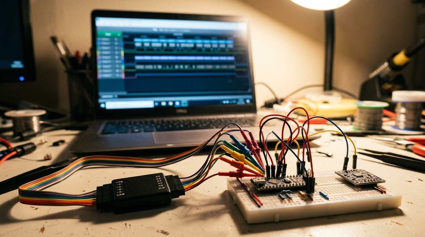
A step-by-step guide to capturing I2C and SPI with an inexpensive USB logic analyzer and sigrok PulseView: signal basics, sampling-rate rules, decoder setup and how to read a decoded transaction.
A sensor board that answers on one microcontroller and stays mute on another is a classic bench puzzle. Printing “device not found” to a serial console tells you that something failed, not where. A logic analyzer records the wires themselves, so the argument about whether the code or the hardware is at fault ends with a captured waveform.
The cheap end of this hobby is well served. Open-source firmware called fx2lafw turns boards built on Cypress FX2 chips into basic logic analyzers, and its supported-device table lists eight-probe Saleae Logic clones among the devices it handles. The PulseView front end then decodes the traffic. The walkthrough below covers the signals, the capture settings and how to read the result. It pairs well with a starter board such as the one in our Elegoo UNO R3 kit review.
What I2C and SPI look like on the wire
I2C uses two lines. SparkFun’s tutorial names them SDA (data) and SCL (clock), and explains that devices can pull a line low but cannot drive it high. Each line therefore carries a pull-up resistor, and SparkFun suggests starting at 4.7 kΩ and adjusting down if needed.
Framing comes from timing relationships, not from extra wires. The NXP I2C specification (UM10204) defines a START as SDA falling while SCL is high, and a STOP as SDA rising while SCL is high. An address follows: seven bits, then an eighth bit for direction, where 0 means write and 1 means read. The receiver acknowledges by pulling SDA low during the ninth clock pulse; if SDA stays high, that is a NACK. Standard-mode tops out at 100 kbit/s and fast-mode at 400 kbit/s, per the same document.
SPI is simpler in framing and heavier in wiring. The sigrok SPI decoder lists CLK as the one required channel, with MISO, MOSI and CS# optional. Chip select is normally held high and pulled low to talk to a peripheral, which SparkFun calls “active low” logic. SPI is full duplex, with separate send and receive lines.
Step 1: pick the hardware and software
Any analyzer that sigrok supports will do. The fx2lafw page reports full support (100 percent) for a long list of eight-probe clones and for evaluation boards built around the CY7C68013A chip. It also warns that some boards marked FX2LP carry the older FX2 part, so check the listing before buying.
PulseView describes itself as a Qt-based GUI for logic analyzers and oscilloscopes. Plug the analyzer in, open the device selector and pick it from the list; if it is missing, the manual says to scan for it first.
Step 2: set the sampling rate
Sampling too slowly is the most common way to capture nonsense. Saleae gives a rule of thumb: sample digital signals “at least 4 times faster than their bandwidth.” For SPI it is blunter: “Always record SPI at least 4x faster than the clock channel.” For a 100 kHz I2C bus, Saleae recommends a minimum of 1+ MSPS, and notes that sampling faster improves timing resolution. Saleae’s sample-rate article is the source for all three statements.
The PulseView manual states a harder floor: the rate “must at least be twice that of the highest frequency you want to capture,” with 3 to 5 times recommended for margin. The two rules agree once margin is applied. Applying the 4x rule to a 400 kHz I2C bus gives 1.6 MS/s as a minimum, and an 8 MHz SPI clock calls for 32 MS/s. That second figure may exceed what a budget analyzer offers; if the rate menu tops out lower, slow the SPI clock in firmware while debugging.
Next, set the number of samples to capture. Press Run, trigger the bus activity from your code, then press Stop.
Step 3: add the decoders
In PulseView, click the add control and choose I²C from the list. The manual says the program tries to match existing signals to the signals the decoder needs; if the match is wrong, a second control lets you reassign SCL and SDA.
For SPI, assign CLK first, then whichever of MOSI, MISO and CS# you wired. The decoder exposes the options cs_polarity, cpol, cpha, bitorder and wordsize. Clock polarity and phase must match the peripheral, and SparkFun notes that the datasheet will specify the sampling edge. Garbled bytes with a clean-looking waveform usually point at that pair of settings.
Step 4: read a decoded transaction
Decoded results appear as annotation rows on the decode signal, with detail visible once you zoom in. The sigrok I2C page shows output lines named Address write, Address read, Data write and Data read, with values such as A0 and A1 in its example. Those are 8-bit forms: the seven-bit address followed by the direction bit, so A0 is a write and A1 a read to the same device.
A typical register read has a recognizable shape:
- START, then an address-write annotation for the device.
- An ACK (or NACK) after the address byte.
- Data write bytes carrying the register number.
- A repeated START, then an address-read annotation.
- Data read bytes, followed by STOP.
The first thing to check is the acknowledge after the address. A NACK there means no device pulled SDA low during the ninth clock pulse.
Reading an SPI exchange
SPI captures read differently, because there is no address byte on the wire. A transaction begins when CS# falls. While it stays low, the clock pulses and the decoder reports one byte per word on MOSI and, at the same moment, one on MISO. That simultaneity is the full-duplex behaviour SparkFun describes: the controller sends and receives in the same clock cycles.
SparkFun notes that the peripheral datasheet indicates whether sending and receiving at the same time is actually possible, so a run of apparent junk on one data line is not automatically a fault. The datasheet also tells you which bytes in each direction carry meaning. When CS# rises, the transaction ends, and any bytes clocked after that point belong to a different exchange.
Zoom out to check the rhythm. As a rule of thumb (opinion, not drawn from the sources), evenly spaced clock bursts, each bracketed by a CS# pulse, point to firmware that is behaving. A CS# that never returns high, or bursts with no pattern, deserves a look at the code that drives the chip-select pin before anything else, and a second capture with a slower clock will show whether timing is part of the story.
Troubleshooting what the capture shows
| What you see | Likely reading | Source basis |
|---|---|---|
| NACK after the address byte | No receiver pulled SDA low on the ninth clock; address or wiring is suspect | NXP UM10204 defines NACK this way |
| Address looks doubled (0xA0 vs 0x50) | The datasheet quotes seven bits; the decoder shows the 8-bit form with the direction bit | NXP: 7-bit address plus R/W bit; sigrok example |
| Unreliable I2C data at a given speed | Pull-up value is a candidate; SparkFun says start at 4.7 kΩ and adjust down if necessary | SparkFun I2C tutorial |
| SPI bytes look shifted or inverted | cpol, cpha or bitorder do not match the datasheet | sigrok SPI options; SparkFun |
| SPI decoder shows nothing | CS# polarity or channel assignment is wrong | sigrok SPI decoder channels and options |
| Edges missing or jittery | Sample rate too low for the clock | Saleae 4x rule |
Treat the middle column as a starting hypothesis rather than a verdict. The capture shows what happened on the wires; the datasheet decides what should have happened.
A habit worth adopting: capture a working device first, even on a different board, and save the file. A known-good trace turns a vague “this looks odd” into a side-by-side comparison. Pi owners can run the same exercise with the Raspberry Pi 5 starter kit as the bus controller.
Sources
- Saleae, “What Sampling Rate Should I Use?”
- PulseView manual (sigrok)
- sigrok protocol decoder: I2C
- sigrok protocol decoder: SPI
- sigrok fx2lafw firmware and supported devices
- SparkFun, “I2C” tutorial
- SparkFun, “Serial Peripheral Interface (SPI)” tutorial
- NXP, UM10204 I2C-bus specification and user manual