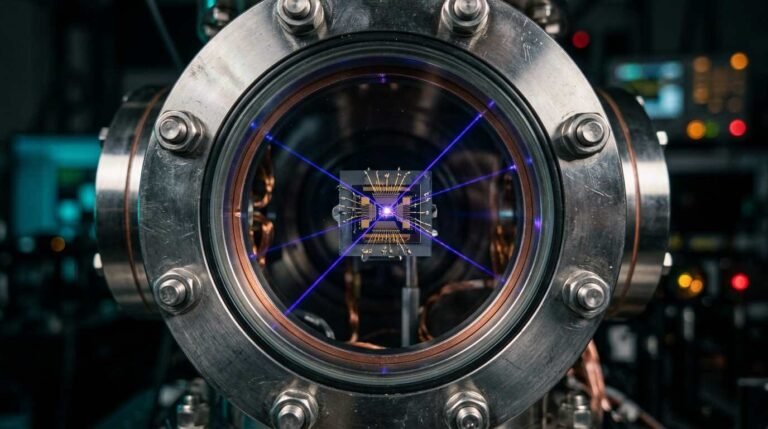






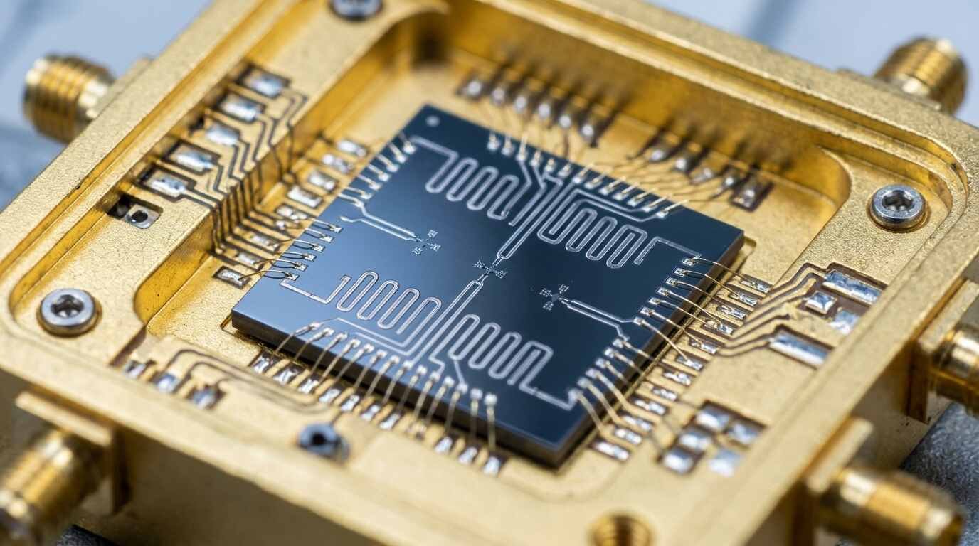
A blinded Fermilab-led study of 22 superconducting qubits links up to twofold swings in transmon qubit performance to oxide, trenches and sidewalls.
Two superconducting qubits drawn from the same design, made from the same niobium film, cooled in the same fridge, can have energy relaxation times that differ by a large factor. A Fermilab-led team in the SQMS Center set out to find why, and the results were summarized by the lab on October 1, 2026. The short version: transmon qubit performance tracks a few nanometer-scale features of the surface and the etched trench around the circuit, and together they account for as much as a twofold spread.
The study is peer reviewed, published in Applied Physics Reviews, and it is unusually frank about what it cannot yet prove. It covers 22 qubits, reports trends rather than statistics, and measures only one kind of loss. That makes it a good paper to read slowly.
The question and why it is awkward
Superconducting transmons are the workhorse of today’s quantum processors. Their useful lifetime is set largely by T1, the time an excited qubit takes to relax, and T1 depends on dissipation in the materials around the circuit. Fabrication teams know that two nominally identical qubits can differ, but that is a nuisance to diagnose, because many things change at once between chips.
The SQMS study tried to separate those causes by working backward. Qubits were measured first. Teams who did not know the T1 results then characterized the devices physically, documenting features before looking for correlations. That blinding is the study’s main methodological virtue, since it reduces the chance that someone finds a pattern because they were looking for it.
The samples
According to the arXiv version of the paper, the set is 22 transmons on seven chips, with four qubits of a common geometry analyzed in depth on several chips. All devices use niobium, about 150 to 200 nm thick, on sapphire or silicon substrates, with aluminum leads and an aluminum oxide barrier forming the Josephson junctions. Some chips have a thin cap of gold, gold-palladium or tantalum over the niobium. Fermilab says the devices came from itself, Rigetti and NIST.
The measurement protocol was long. Each qubit’s T1 was tracked continuously for 10 hours in a single cooldown, so that package, readout coupling and radiation environment are roughly shared. The authors saw no dependence of T1 on a qubit’s position on the chip.
Three features that stood out
The first is trench depth. Circuits like these are etched into the substrate as well as the metal, leaving a trench under and beside the film. Quality factor rises with trench depth, with the largest variation below about 20 nm. Simulations show surface loss falling roughly logarithmically with depth and saturating near 70 nm; beyond that, depth no longer correlates with quality factor. Sapphire trenches in this study were limited to 15 to 20 nm, so they sit in the sensitive range.
The second is the sidewall angle at the foot of the metal. A smoother decline from metal top to substrate trended with lower quality factor. Electromagnetic simulation gives a surface participation ratio 15 to 20% higher at about 30° than at 10 to 15°. Fermilab’s summary of the same result says a sharper angle predicts a 20 to 30% improvement. Those are not the same statement, and I flag the difference below.
The third is surface niobium oxide. On one bare-niobium chip the oxide thickness varied from about 5 to 7 nm across the chip, a spread of only 1 to 2 nm, and thicker oxide went with lower quality factor. Fermilab’s summary notes that single-nanometer variations can shift performance meaningfully. Together, the lab says, these three features account for as much as a twofold variation among qubits made from identical materials.
Working through the numbers
The paper’s headline metric is quality factor, Q = 2π f T1, where f is the qubit frequency. Take Qubit 1 on Chip 1: T1 averages 116 µs at 4.726 GHz. Then Q = 2π × 4.726 × 10⁹ × 116 × 10⁻⁶, which is about 3.44 × 10⁶, matching the paper’s table. Qubit 2 has T1 of 94 µs at 4.078 GHz, giving 2.41 × 10⁶, and Qubit 3 has 109 µs at 4.158 GHz, giving 2.85 × 10⁶.
The ratio of the best to the worst of those three is 3.44 over 2.41, about 1.43 in Q. Using Q rather than raw T1 matters here: the T1 ratio is only 116 to 94, or 1.23, but the qubits sit at different frequencies, and for a given Q a higher-frequency qubit has a shorter T1. Comparing Q takes the frequency out.
Loss is usually discussed through the surface energy participation ratio, or EPR, the fraction of the electric field energy stored in a lossy layer. The paper’s simulations show the surface EPR roughly doubling, from about 2.8 × 10⁻⁵ to 5.8 × 10⁻⁵, when the oxide grows from 5 to 10 nm. An EPR is converted to a loss by multiplying with the material’s loss tangent, which the authors take as about 0.1 from earlier cavity measurements. I have not done that multiplication here, because the simple product does not reproduce the measured quality factors, and the paper does not claim that it should. The EPR is useful as a relative guide, not an absolute prediction.
Undercuts, exposed niobium and the other chips
The sidewall story has a refinement. Simulations in the paper suggest that an undercut of about 60 nm beneath the metal edge can reduce surface participation by 50 to 75%, because it pulls electric field away from the lossy oxide. Shallow undercut angles, however, can trap field and raise the participation again. Lithography teams can in principle tune both the angle and the undercut, which makes this a rare finding that points straight at a process knob.
On the chip capped with gold-palladium, a strip of niobium about 100 nm wide stays exposed near the sidewall and oxidizes, and longer exposed strips trend with lower quality factor. That is consistent with the oxide picture but is a different mechanism from simple thickness, because it concerns where the oxide sits. On the same chip the sidewall oxide itself varies by only 0.5 to 1 nm and shows no clear correlation.
For context, the paper cites T1 ranges from other groups: 215 to 323 µs, 312 to 476 µs, 152 to 270 µs and 42 to 113 µs in four earlier reports. The Chip 1 values here, 94 to 116 µs, fall toward the lower part of that spread. I did not open the cited papers, so these are the SQMS authors’ comparisons, not verified independently. The relevance is that a twofold spread matters more when the baseline is modest.
What turned out not to matter, or not yet
Several suspects were cleared, at least provisionally. Scratches, particles and lithographic defects showed no clear correlation with performance. The junction chemistry looked the same by electron microscopy, and the aluminum grain size, the normal-state resistance and the switching current showed no clear trend. Impurities in the time-of-flight mass spectrometry data, including carbon, hydrogen, oxygen, chlorine and fluorine, followed no consistent pattern, though the authors say fluorine may matter and needs more statistics.
Niobium hydrides, a long-standing concern in niobium cavities, also showed no consistent trend in this set. Sidewall oxide thickness varied only 0.5 to 1 nm and did not correlate, which is as much a statement about the small variation as about the physics.
Two possible shortcuts for screening chips
The paper proposes two low-temperature techniques as proxies for qubit performance, which would be valuable because measuring a qubit requires a full dilution-refrigerator cooldown. Terahertz near-field spectroscopy produces a signal intensity that scales with trench depth. Magneto-optical flux imaging at 4 K shows that the total area penetrated by magnetic flux scales inversely with quality factor, for applied fields of 80, 100 and 120 oersted. The authors say the mechanism is not yet understood.
Both are preliminary. The terahertz simulations are still in progress, and a proxy measurement that cannot be explained is a lead, not a screening tool. Still, a method that tells you something about T1 before cooling the chip would save weeks.
Limits of the claim
Twenty-two qubits is a small sample. Several trends are chip-specific; the bare-niobium chip does not follow the trench-depth trend. The three features together do not fully explain the observed spread, and the paper reports no correlation coefficients or statistical tests, only trends read from scatter plots. The 20 to 30% and 15 to 20% figures are simulation outputs, not direct measurements of qubit improvement.
The study also covers only T1. Dephasing and T2 coherence are the stated next step, along with controlled A/B experiments that change one feature at a time. Fermilab’s own words call the work the beginning rather than the end. A fair summary is that it supplies a ranked list of suspects, with the strongest evidence for a thin surface oxide, a deep trench and a steep sidewall.
A practical reading: because the three features act through the same mechanism, loss in a thin oxide layer near the metal edge, they are partly interchangeable. A deeper trench can compensate for thicker oxide, to the extent that the simulations hold. That is another reason the paper’s authors want controlled experiments before drawing a ranking.
Frequently asked questions
What is T1 in a transmon qubit?
T1 is the energy relaxation time, the typical time an excited qubit takes to decay to its ground state. Longer T1 generally means less dissipation in the qubit’s materials.
How much did the features change performance?
Fermilab reports that trench depth, oxide thickness and sidewall angle together account for as much as a twofold variation in performance among qubits made from identical materials.
Was the study peer reviewed?
Yes. Fermilab cites Applied Physics Reviews, volume 13, issue 2, article 021416. The earlier arXiv version, number 2503.14424, was the source for the detailed numbers here.
Does this mean the cause is proven?
No. The paper reports correlations from 22 devices and says controlled experiments are future work. It does not report formal correlation coefficients.
The practical value of this paper is that it shortens the list. Instead of blaming an undifferentiated fabrication process, a foundry can now check three specific things: how deep the trench is, how steep the sidewall is, and how thick the native oxide has grown. If those checks are cheap, a chip can be rejected before a cooldown. What remains is the harder question of why a 1 to 2 nm change in oxide matters as much as it seems to, and whether T2 will tell the same story as T1. Until the controlled experiments arrive, treat the trends as strong hints and the simulated percentages as estimates.
Sources